

When NVIDIA pulled NVLink off consumer GeForce cards starting with the RTX 40-series, the marketing line was polite: die area for “AI features,” gamers do not need multi-GPU bridges, PCIe 5.0 ×16 is “plenty.” That story is incomplete. What actually happened is a product-line partition. Fast GPU-to-GPU fabric stayed on the enterprise side of the wall. The home lab, the indie inference box, and the small hosting shop were invited to “mess around” on a host bus that was never designed to be a multi-accelerator memory fabric.
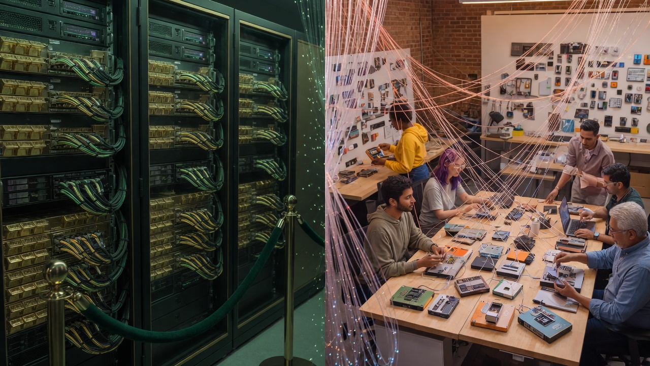
What NVLink was — and who still gets it
NVLink is a high-bandwidth, low-latency link between accelerators. On earlier GeForce high-end cards (notably the RTX 2080 Ti class and the RTX 3090), enthusiasts could still bridge two boards and move tensors without slamming every byte through the CPU’s PCIe root complex. With Ada Lovelace (RTX 40), those connectors disappeared from GeForce. Blackwell consumer cards did not bring them back. The bridge did not vanish from NVIDIA’s roadmap — it moved upstairs.
On the corporate side, NVLink kept evolving. Hopper and Blackwell data-center GPUs sit in NVLink domains (HGX, DGX, GB200-class NVL systems) where peer bandwidth is measured in terabytes per second across a GPU complex, not in the tens of gigabytes per second a single PCIe 5.0 ×16 slot can sustain end-to-end under real protocol overhead. That is the difference between:
- Tensor-parallel inference and training that treat multiple GPUs as one memory-coherent-ish machine, and
- PCIe-bound multi-GPU, where every cross-card gradient, KV-cache shard, or all-reduce fights the host bus, the chipset, and NUMA.
PCIe 5.0 ×16 is a fine upgrade for a single fat GPU talking to NVMe and NICs. It is a poor substitute for a purpose-built accelerator fabric when you want many GPUs to behave as one brain. Calling that “good enough for home users” is not generosity. It is market segmentation with a smile.
The real customer of NVLink 5
Enterprise NVLink (including the NVLink 5 generation on Blackwell-class systems) exists so hyperscalers, national labs, and well-funded AI companies can deploy real multi-GPU inference and training: large contexts, expert parallelism, tight collectives, rack-scale “one logical GPU” designs. Those buyers pay for SXM modules, liquid cooling, NVIDIA networking, and software stacks that assume the fabric is there.
Meanwhile the builder with two or four GeForce cards in a tower is told the future is:
- Buy more VRAM on a single card (until the MSRP looks like a car payment), or
- Accept PCIe as the interconnect and watch utilization graphs lie about “multi-GPU,” or
- Graduate to enterprise SKUs — if export rules, power, and budget allow.
That ladder is not an accident. A closed, premium fabric turns multi-accelerator competence into a class marker. The rich cats get the bus. Everyone else gets a slot.
When the fast path is only on the quote that requires a sales engineer, “democratizing AI” is a slide deck, not a product policy.
Huawei’s constraint — and the open counter-move
Huawei’s situation is different and, bluntly, harsher. Advanced process nodes and some Western GPU ecosystems are restricted. You cannot casually buy your way into the same closed ladder. So the company did something both necessary and ingenious: invest in scale-out interconnect and architecture so that many NPUs can act as one machine — SuperPoDs and SuperClusters — instead of pretending a single sanctioned-node chip will win on peak FLOPs alone.
The protocol behind that push is UnifiedBus (UB). Atlas 900 A3 SuperPoD deployments already run on UnifiedBus 1.0 at meaningful customer scale. At HUAWEI CONNECT 2025, Huawei released the technical specifications for UnifiedBus 2.0 and positioned it as openly accessible for industry partners: bus-grade interconnect, peer-to-peer coordination, resource pooling, and a path to thousands of NPUs working as one logical computer. Companion directions include UBoE (UnifiedBus over Ethernet) so clusters can ride familiar switching where that fits, alongside the pure SuperPoD fabric story.
Is that pure altruism? No — and it does not need to be. Huawei has said clearly that AI monetization stays centered on hardware, while opening software stacks (CANN interfaces, Mind toolchains, foundation-model lines on stated timelines) and interconnect specs to grow an ecosystem. Necessity forced the architectural bet; openness is how you turn a constrained supply chain into a shared standard instead of a private cage.
That is the opposite instinct from locking the best GPU-to-GPU path behind enterprise SKUs and telling everyone else to enjoy PCIe.
The memory wall is scarier than the node race

Interconnect politics matter. Something more fundamental still sits underneath both NVLink and UnifiedBus: the memory wall.
For years the industry story has been miniaturization — smaller transistors, denser logic, more FLOPs per watt on the slide. That race is real, and it is expensive. But modern AI workloads are often not limited by how cute the multiply-accumulate is. They are limited by how fast you can move weights, activations, and KV cache to the arithmetic units that are already starving. A brilliant compute die with a thin straw to DRAM is a Borg cube with no power couplings: intimidating silhouette, empty interior.
The wall has layers:
- Off-package DRAM — HBM helps, but capacity and channels still bound the design.
- On-package and on-die SRAM — fast, tiny, and never large enough for frontier contexts alone.
- Chip-to-chip and host paths — PCIe, CXL, and even premium GPU fabrics become the next straw once local memory is exhausted.
You can win a node race and still lose the workload if every token pays a memory tax. That is why “just shrink the process” is an incomplete strategy for inference at scale — and why export pressure on advanced lithography does not automatically freeze out anyone who can stack, via, and wire memory next to compute.
Chinese packaging and 3D integration work — including aggressive use of TSVs (through-silicon vias) and multi-layer chip stacking — is aimed squarely at that wall. Short vertical paths replace long horizontal treks across a package or board. Logic and memory (or multiple logic tiers) sit in a volume instead of a postcard. Bandwidth and energy per bit improve because the physics of a via through stacked silicon is kinder than another trip out to distant DRAM over a conventional path. Done well, stacking does not merely decorate a process-node lag — it can sidestep the memory wall’s worst geometry in a way that pure planar shrink does not.
That may be more fundamental than the next nanometer brag. Miniaturization still matters for density and power. But if the bottleneck is feeding the cores, the scary cube is not “who has the smallest gate.” It is who builds a monolithic-enough memory-compute organism that the cores never wait. Open scale-out buses (UnifiedBus and kin) attack the wall between packages and racks. TSV stacking attacks the wall inside the package. Together they are a different theory of victory than “only the richest get NVLink and only the smallest node gets to play.”
Western roadmaps know this too — HBM stacks, advanced packaging, and fabric-heavy systems are memory-wall responses with different branding. The point is not nationalism as physics. The point is priority: when memory movement dominates, stacking and open multi-accelerator wiring can outrank a pure miniaturization cult — especially for players who cannot buy the latest EUV lottery ticket every year.
People vs. rich cats — the interconnect test
Judge the vendors by who may link accelerators, not by who ships the flashiest single-die demo.
| NVIDIA consumer path | NVIDIA enterprise path | Huawei SuperPoD path | |
|---|---|---|---|
| Fast GPU/NPU fabric | Removed from GeForce (40-series onward) | NVLink generations through NVLink 5 domains | UnifiedBus 1.0 → open UB 2.0 specs |
| Home / small lab multi-accelerator | PCIe 5.0 ×16 and hope | Not the target SKU | Architecture aimed at many chips as one machine |
| Who the fabric optimizes for | “Mess around” on the host bus | Corporate and cloud inference/training at scale | Partners building SuperPoD-class systems on open specs |
| Openness of the interconnect story | Closed; GeForce cut off | Closed product + software moat | UB 2.0 specs released for industry adoption |
NVIDIA’s move concentrates capability where the invoices are largest. Consumer silicon still trains LoRAs and runs local chat — until the model, context, or parallelism needs a real fabric. Then the ceiling is sudden and expensive.
Huawei’s move, forced by geopolitics and process limits, still points the other way: if you cannot win only on the fanciest transistor, you win by wiring many competent accelerators together and publishing enough of the bus that others can build on it. That is infrastructure for an industry, not a velvet rope around a club.
Call it plainly: Huawei is playing a people-scale interconnect game — open the bus, scale the pod, monetize metal. NVIDIA is playing a rich-cat fabric game — keep NVLink where the capital expenditure lives, and let the home rack discover that PCIe is a driveway, not a highway.
What this means if you actually host and ship systems
For operators and builders who care about sovereignty and cost:
- Do not confuse a GeForce shopping cart with a multi-GPU architecture. Two beautiful cards in one chassis are not an NVLink domain.
- Measure collectives and KV movement, not only tokens/sec on a single device. The fabric shows up in the traces.
- Watch open interconnect specs (UnifiedBus 2.0 and whatever honest alternatives emerge). Standards that survive outside one vendor’s premium SKU list are how smaller players stay in the game.
- Plan power, cooling, and software for the bus you can actually buy — and be honest when the bus you need is gated.
Closing
Removing NVLink from RTX 40-class GeForce was not a gift of extra AI transistors to gamers. It was a clean cut between hobby multi-GPU and production multi-GPU. NVLink 5 and its enterprise cousins are there so corporate buddies can deploy serious inference and training. PCIe 5.0 ×16 is what is left when you are not on that list.
Huawei, blocked from the easy path, open-documented UnifiedBus 2.0 so very large numbers of NPUs can be linked as one system — necessity sharpened into an ecosystem bet. One side walls off the fast path. The other publishes the bus.
If “AI for everyone” is more than a keynote slogan, the interconnect policy is the tell. Watch who gets the fabric — and who is told the slot is enough.
Building or hosting AI infrastructure and want a second opinion on fabric, power, and ops reality? Talk to 3DN.

Leave a Reply